Physical Design Engineer
Reference: JOB-1040
Looking for Physical design engineer for Bangalore location
Major responsibility
Own block-level and/or subsystem-level implementation from RTL to signoff-clean GDSII on advanced FinFET / GAA nodes.
Role
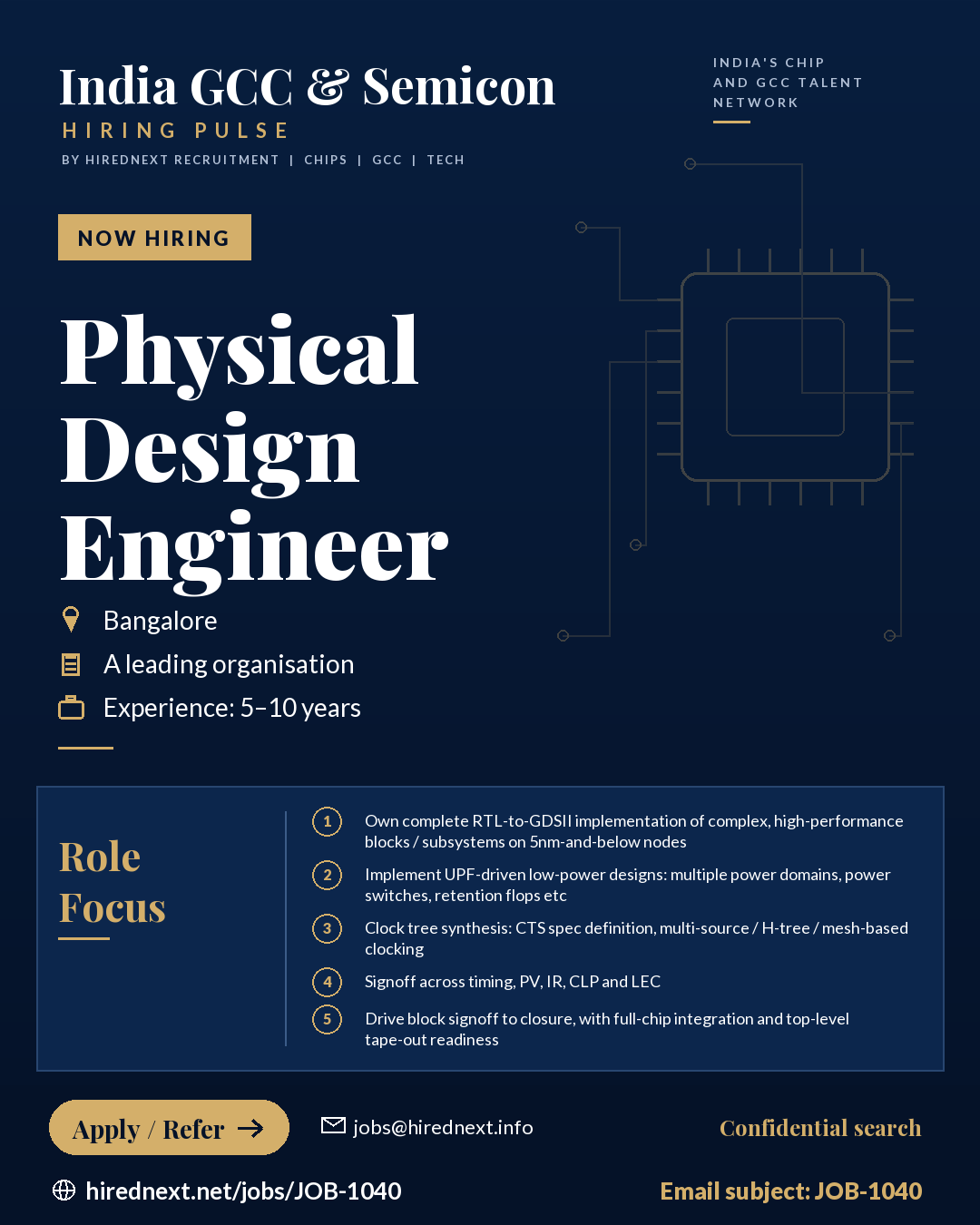
- Own complete RTL-to-GDSII implementation of complex, high-performance blocks / subsystems on 5nm-and-below nodes
- Implement UPF-driven low-power designs: multiple power domains, power switches, retention flops etc.
- Clock tree synthesis: CTS spec definition, multi-source / H-tree / mesh-based clocking
- Signoff across timing, PV, IR, CLP and LEC
- Drive block signoff to closure, with full-chip integration and top-level tape-out readiness
- Scripting (Tcl / Python / Perl) and automation to improve QoR and turnaround time
Key skills: PD, Physical design engineer
Apply
Apply via the form below, or email your CV to jobs@hirednext.info with the exact subject JOB-1040 so it reaches the right role. Client details remain confidential. HiredNext never charges candidates to apply.
Similar opportunities
Apply for Physical Design Engineer
Your application is submitted only for this exact role. Make sure your CV presents the experience and impact most relevant to this mandate.
Does your CV clearly show that you match this JD?
Optional support. Applying is free. Purchasing any service does not influence shortlisting or guarantee an interview.
This is an optional paid professional service. It is separate from your job application and does not affect shortlisting.
No thanks — continue to all jobs →